In this chapter, the current state of the art of integrated (silicon) photonics is going to be outlined. In recent years, new computational methods to explore the vast parameter space of even compact photonic devices have been developed. The inverse photonic design approach, which is one such method, will be explained thereafter. Lastly, the challenges and opportunities of graphene integration into PICs will be discussed.
Optical Link
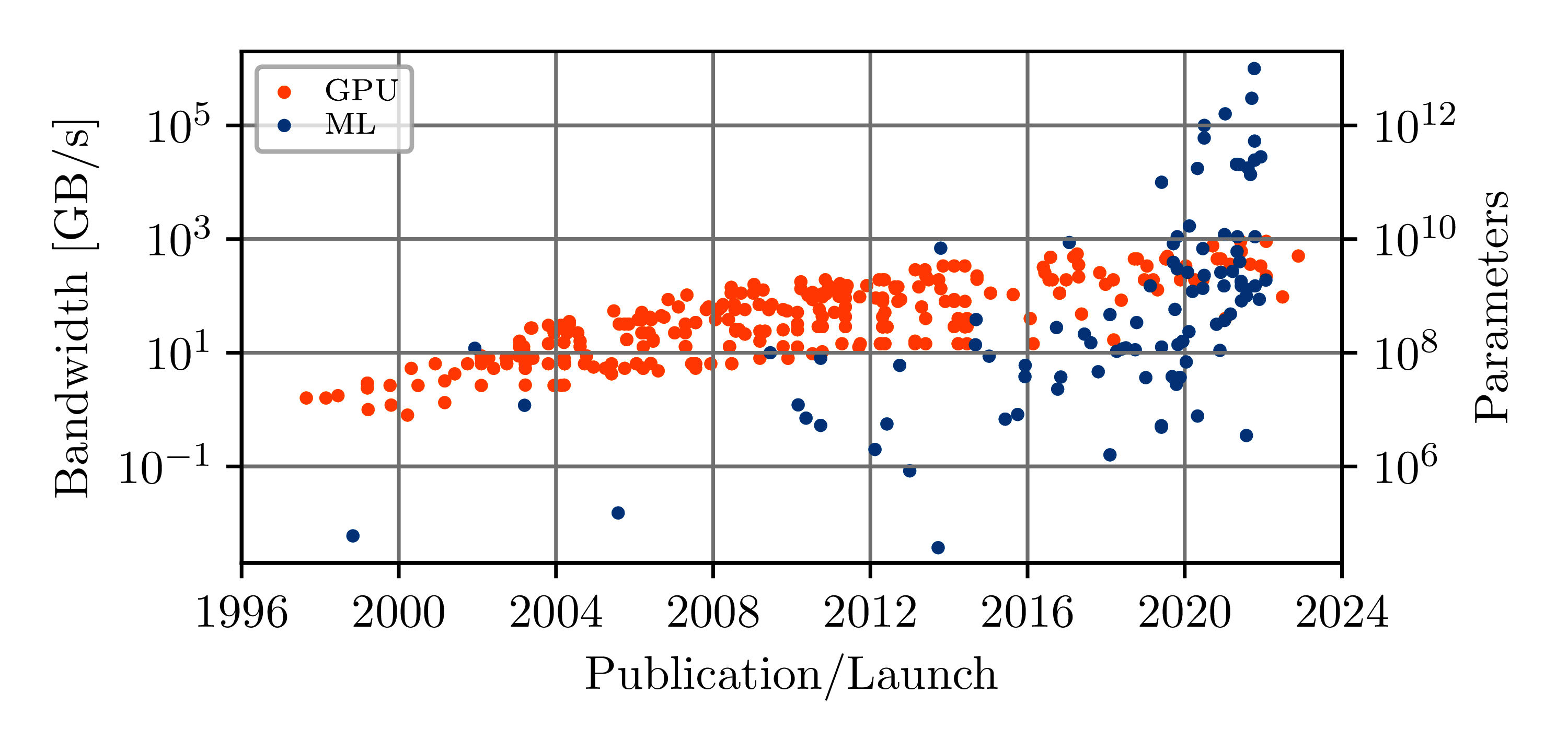
Figure 1:Scaling of the total memory bandwidth of Nvidia GPUs over their release date (orange) based on List of Nvidia Graphics Processing Units, 2022. Number of trained parameters of scientifically relevant ML-models by their publication date (blue) Villalobos et al., 2022. Note that for both the bandwidth and the number of training parameters the scale is two decades per division.
The memory bandwidth scaling of modern GPUs does not keep pace with the explosion in ML model size (see Figure 1). The resulting data bottleneck can potentially be lifted by optical chip-to-chip communication Hosseini et al., 2021.
Optical data connections already form the backbone of the modern information era. The distances at which optical links are used have scaled to short-reach data center connections over the last twenty years and first demonstrators for chip-integrated transceivers have been put forward Sun et al., 2015.
\begin{figure}[b!]
\centering
\includesvg[width=\textwidth]{sections/Introduction/assets/optical_link/Link_pic_to_pic_small_no_text.svg}
\caption{Simplified architecture of a single optical link between distant electronic ICs. Both the photonic TX and RX are deposited in the BEOL, which is enabled by using graphene as the active material. }
\end{figure}\label{fig:link_overview}
An optical communication link (see figure ) consists of three major components, the transmitter, the transmission medium, and the receiver. This subsection describes the constituents of these components. The optical link investigated here connects two electronic ICs by a BEOL integrated photonic layer. On the transmitting side \qty{1550}{nm} light is first generated by a laser, which can provide a single or multiple carriers depending on whether WDM is used. For the sake of simplicity, a single non-multiplexed OOK link is considered here. The laser light is coupled to the photonic layer of the transmitting IC via a low-loss coupler, where it is selectively attenuated by the modulator depending on the data stream. The modulator is driven by a chain of inverters of increasing size Pantano et al., 2020.
Subsequently, the amplitude-encoded light is guided to the receiving IC via integrated waveguides, two additional couplers, and some length of optical fiber. At the receiver, the light intensity is converted to a photocurrent/voltage by a photodetector. The efficiency of this conversion is expressed by the detector's responsivity . Typically the generated current is amplified to a detectable level using a TIA.
The maximum rate at which data can be transmitted over the link is determined by ISI or distortion and noise. In this work, ISI is assumed to be dominated by the bandwidth of the modulator and detector, due to their short distance suppressing dispersion effects Djordjevic, 2022[ch. 2.4.2].
Sources of noise in optical links
Noise probabilistically shrinks the separation between the \on and \off levels at the receiver making it harder to determine the level with certainty. This is expressed in terms of the link quality factor Venghaus & Grote, 2017[ch. 6]:
Where and are the power in the \on and \off state respectively.[1] and denote the standard deviation in the respective state, which is introduced by noise. Q directly determines the BER Venghaus & Grote, 2017[ch. 6]. Every component of a link contributes to the overall noise. However, the analysis can oftentimes be limited to the dominating noise terms. Sources of noise and distortion are summarized in table \ref{tab:noise}. \input{sections/Introduction/noise_table.tex}
Silicon Photonics
This section is going to give a brief introduction to state of the art of integrated photonics. It will provide an overview of typical passive photonic devices, like waveguides, couplers, and (selective) splitters, thermal phase shifters and state-of-the-art of detectors. This section is not going to introduce modulators in-depth, as these will be dealt with in great detail in the subsequent section. Throughout this section, the transmission characteristics expressed in terms of S-parameters of the different devices will be provided.
Passive Devices
In electronics the distinction between passive and active devices is typically made based on their energetic behavior: If the time integral over the instantaneous power cannot be negative, with the integral starting at a time, when no electrical energy is present in the system, the device/network is considered passive https://www2.dke.de/de/Online-Service/DKE-IEV/Seiten/IEV-Woerterbuch.aspx?search=151-11, undefined[131-11-34]. This definition differentiates active and passive devices by their ability to generate electrical power. In photonics on the contrary a definition based on the ability to control the electrical/optical power flow by an external input is typically employed. Therefore apart from photodetectors also electro-optical modulators and thermal phase shifters are considered active photonic devices, despite their inability to generate power.
Waveguide
The fundamental building block of every PIC is a waveguide, which enables to force the flow of light along a predetermined path. The most common waveguides in silicon photonics are based on a combination of at least two dielectric materials with different refractive indices called dielectric waveguides Doerr & Kogelnik, 2008. Other waveguide architectures include photonic crystal Joannopoulos, 2008 waveguides and plasmonic waveguides Ding et al., 2020.
In dielectric waveguides, the higher refractive material forms the core, which is surrounded by the lower refractive index material, called the cladding. This cross-section extends invariantly along the direction of propagation. Due to this arrangement light can be confined in and around the core region by total internal reflection (see box). In such a translation invariant waveguide depending on the waveguide cross-section there can exist one or more orthogonal eigenmodes fulfilling Maxwell's equations Reider, 2013. Analogous to the propagation of plane waves in free space the field distribution along a waveguide can be described by the equation of propagation by replacing the wave vector with the propagation constant Meschede, 2015:
Where is the frequency (in ) of the harmonic oscillation of the - and -fields. While for a lossless waveguide is purely imaginary, in a lossy waveguide becomes complex-valued. The factor is used in this work so that the power in a waveguide decays with:
Splitters and Couplers
It is frequently necessary to divide, combine, and couple optical power from one waveguide to another, e.g. to construct an interferometer. An overview of photonic splitters and couplers is given in appendix \ref{ap:splitters}. \begin{figure}[h] \includesvg[width=\textwidth, inkscapearea={page}]{more_passives.svg} \caption{Selection of passive integrated photonic devices. (a-b) Show MMIs having a single (a) and two (b) inputs, compared to directional couplers (c) the splitting ratio of MMIs is highly balanced Romero-García et al., 2013. Y-junctions (d) exhibit a similar property. However, no 2x2 equivalent exists. Find a more detailed description of those devices in appendix \ref{ap:splitters} (e-f) Show Bragg and Sagnac reflectors respectively Chrostowski & Hochberg, 2015.} \end{figure}
Reflectors
A commonly required functionality (e.g. to build resonators: see section Resonators) is the complete or partial reflection of light into its counter-propagating mode. Apart from resonant reflectors, which will be covered in detail in section Resonators, other device architectures include multimode interferometer reflectors Xu et al., 2009 and Sagnac loops Jiang et al., 2016Zhang et al., 2014Wu et al., 2017, which split the light in a MMI, directional coupler or Y-junction route the light in a loop and combine it using the same component used to split the light. The light travels along the same path in different directions and thus acquires the same phase. Therefore, it will in any case arrive at the combiner with an unchanged phase difference compared to it exiting the splitter. In the case of a Y-junction or 1x2 MMI, this phase difference is 0. All the light will be scattered back. Consequently the (only) S-parameter has a magnitude of 1 and a phase determined by the round trip phase accumulated in the loop. Using a balanced 2x2 splitter the light is fully reflected into the waveguide it originated from: .
Active Devices
Most modern logic is based on electronics, it is thus highly desirable to control photonic circuits using electrical signals. Active devices enabling the conversion between electrical (control) signals to optical properties/signals and back are widely adopted and form the backbone of today's fiber optic telecommunications.
Thermal Phase Shifter
Slow phase shifters are used to compensate for fabrication inaccuracies and environmental changes (e.g. the environmental temperature, humidity, etc.) and to enable reconfigurability (photonic FPGAs). For slow phase shifting in silicon photonics, typically the thermo-optic coefficient of dn/dT = \qty{1.8e-4}{\per\K} at \qty{300}{\K} Komma et al., 2012 is leveraged.
It has been shown, that graphene is a suitable heater material due to its high electrical and thermal conductivity and its comparably low optical loss Hu & Wang, 2018. The optical loss could further be reduced by doping the graphene.
Detectors
As discussed in section a photodetector is required in any optical link to convert the signal back from the optical to the electrical domain. Typical performance metrics of photodetectors are its conversion bandwidth, responsivity and required bias. describes the conversion efficiency from optical power to photo-current . Diverse physical effects can be used for this conversion. However, most commonly electron-hole pair generation and separation in reverse-biased PIN diodes are used. Optically active transitions must be possible in the used material, to enable photo-absorption. For the O- and C-band this is not the case for silicon, due to its bandgap (\qty{1.12}{eV}) exceeding the photon energy E_{ph}=h\nu=\qty{0.8}{eV}@\qty{1550}{nm}=\qty{0.94}{eV}@\qty{1310}{nm}. Germanium has a smaller bandgap (\qty{0.67}{eV}) enabling its use as a photodiode at the communication wavelength. It can be monolithically integrated into standard CMOS process lines. Consequently, it became the workhorse for silicon photonics. The state of the art of germanium photodiodes is rapidly evolving. While the reported \qty{3}{dB} bandwidths were not surpassing \qty{120}{GHz} ten years ago Vivien et al., 2012Lischke et al., 2015Lischke et al., 2017 a record high bandwidth of \qty{265}{GHz} was demonstrated last year Lischke et al., 2021. The reported responsivities range from \qty{0.3}{A/W} to \qty{1}{A/W} Lischke et al., 2015, which is relatively close to the quantum conversion limit of R_{opt} = \frac{e}{h\nu} = \qty{1.26}{A/W}. Other high speed photodetector technologies demonstrating more than \qty{100}{GHz} bandwidth are graphene and InPBach et al., 2004Beling & Campbell, 2009. Graphene photodetectors have shown to support bandwidths of up to and potentially more than \qty{130}{GHz} Ding et al., 2020Schall et al., 2018Ma et al., 2019Ding et al., 2020 and optically broadband absorption. The reported responsivities vary vastly from single digit mA/W Schall et al., 2014Fang & Hu, 2017 in pure graphene devices and hundredsGosciniak & Khurgin, 2022 or even several millions of A/W Liu & Kar, 2014Liu et al., 2017 in photodetectors using plasmonic enhancement or graphene silicon heterojunctions respectively. The responsivity of graphene photodetectors is reported by some groups in terms of as graphene photodetectors typically generate a voltage rather than a current Schuler et al., 2021Liu & Kar, 2014.
Modulators
In this section EO phase modulators and EA modulators will be introduced. Furthermore, an overview of commonly used performance metrics and their applicability to different types of modulators will be summarized.
Performance Metrics
The following performance characteristics are of high relevance to optical modulators. Should a modulator technology not be able to fulfill the requirements with respect to these metrics dictated by the optical link it is supposed to be used in, it is infeasible for the respective link.
A modulator has to switch states with high repetition rates, which is typically characterized by its \qty{3}{dB} \textbf{EOBW}, indicating the frequency at which the power transmission from the electrical to the optical domain drops to half of its initial value at low frequencies.
Modulator bandwidth limitations typically stem from the charging time constant of some capacitor (diode depletion region, graphene insulator graphene/silicon, silicon slot, etc.) contacted via some amount of access resistance forming an RC-lowpass Phare et al., 2015Ding et al., 2010. Other limitations include carrier lifetimes Zhou et al., 2008, coupling rf power to the substrate Lederer & Raskin, 2003, phase mismatch in traveling wave devices Witzens, 2018, and photon lifetimes in resonant devices Sacher et al., 2012. The ratio of transmission between the transparent and absorptive state in a modulator is characterized by its \textbf{MD} (also called ER) defined as Koester et al., 2012:
\label{eq:md} Where () is the transmitted field in the transmissive (opaque) state. an denote the power transmission in the respective states. A specified amount of MD is typically required in a communication link to allow for operation not surpassing a specified BER. A high MD is beneficial for the links -factor and thus BER in multiple ways: It leads to an increased separation in power levels at the receiver. Simultaneously it suppresses the optical noise power in the off state, reducing the overall noise at the receiver. In tandem to MD the \textbf{IL} is defined by the remaining loss introduced (inserted) by the modulator in its transparent state Heuermann, 2018:
\label{eq:il} It should be noted that the definition of the sign of IL is ambiguous. Graphene however generally does only introduce loss and no gain. In this work, IL will be defined such that it has a positive sign for lossy structures. Both IL and MD can be normalized by the interaction length of the modulator Sinatkas et al., 2021. Another highly regarded metric for modulators is their power consumption, which is typically expressed in terms of \textbf{energy per bit}. Naively the energy per bit of a modulator is determined as the average energy required to charge and discharge the modulator capacitorMiller, 2012Witzens, 2018Koester & Li, 2014Koester et al., 2012:
Here is the total modulator capacitance and is the peak-peak voltage applied to the modulator to enforce switching. The factor is a consequence of the fact, that for a random or pseudo-random bit pattern the capacitor undergoes a full charge cycle every 4 bits on average Koester et al., 2012. One full charge cycle requires an energy of , half of which is used to charge the capacitor, while the other half is dissipated in the series resistance during the charging process Miller, 2012.[2]
A figure of merit commonly considered for EO modulators is the product of the voltage required for a phase shift and the device length . This figure of merit represents an inherent trade-off between footprint and required drive voltage, characterized by the strength of interaction of the light with the active medium Ding et al., 2010Sorianello et al., 2018. However, in EA modulators the LMI is typically expressed in terms of \textbf{absorption} (or modulation) \textbf{per unit length} Mohsin et al., 2014Koester & Li, 2014. A detailed overview of Si, SiGe and Graphene modulators can be found in reference Hu et al., 2016 and a comparison additionally including LiNbO3, InGaAsP/InP in Romagnoli et al., 2018. An overview of IL and MD of state-of-the-art EA-modulators is provided by Sinatkas et al., 2021. The comparison is shown in figure with the addition of Mohsin et al., 2014. \begin{figure}[h] \centering \includegraphics[width=0.6\textwidth]{compare_modified.pdf} \caption{Overview of MD and IL of state-of-the-art EA-modulators color-coded by their active medium. Mohsin et al. (2014) reported the highest MD/IL ratio of graphene EA-modulators to this date. The original diagram Sinatkas et al., 2021 was modified to include this data point.} \end{figure}\label{fig:md_il_overview}
Resonators
An improvement in the mentioned performance metrics is oftentimes accomplished by the use of an optical resonator Romero-García et al., 2017Witzens, 2018. The fundamentals and possible implementations of optical resonance will be discussed in the following.
Optical Resonance
Under constructive interference of repeated reflection (recycling) of light, a strong enhancement in the intensity can be observed. This phenomenon is called optical resonance and has diverse use cases such as switching Nojić et al., 2020, filtering Wang et al., 2022, modulation Witzens, 2018, lasing Xiang et al., 2022, sensing Claes et al., 2009, comb generation Chang et al., 2022 and isolation White et al., 2022. In this work, it will be evaluated whether optical resonance can be leveraged to overcome the trade-off between MD and IL inherent to EO modulators (see section Rectlinear Modulator). Defining characteristics of a resonator are its resonant frequency and the decay of its stored energy over time (ring down), which is described by its cavity lifetime as:
Where is the power exiting the resonator. From this first-order differential equation, it becomes clear, that decays exponentially as:
Where is the stored energy at time . A representation of decay, which is not dependent on the timescales at which the resonator oscillates is found in the dimensionless quality factor defined as:
Which has a FWHM of:
By describing the ring down in terms of an oscillation with exponentially decaying amplitude and taking the squared Fourier transform one finds the PSD to have a Lorentzian shape:
Fabry-Pérot and Ring Resonator
The two most broadly adopted ways to create an optical resonator are the Fabry-Pérot and ring resonators. A Fabry-Pérot resonator is created by placing two reflectors such that the light is repeatedly recycled between them. One or both of the reflectors can be made partially transmissive (see fig. (b-h)), to couple light out of such a resonator. The ring type of resonator involves guiding the light in a closed loop. Waveguides are well suited for this application and allow for ring resonators of micrometer size Xu et al., 2008. Coupling to and from waveguide ring resonators is typically performed using the evanescent overlap between adjacent waveguides (see fig. (a)). The main difference between the two architectures is that in the Fabry-Pérot type the forward and backward traveling waves take the same path, leading to a standing wave pattern Hodgson & Weber, 2005, which is not the case in ring resonators. Furthermore, the propagation section in integrated Fabry-Pérot resonators can be made short enough to support the fundamental resonator mode at optical/NIR frequencies Chrostowski & Hochberg, 2015, while this is theoretically possible for ring (disk) resonators, such resonators suffer from high radiation loss Xu et al., 2008. It can be shown, that apart from such practical differences the transmission behavior of linear Fabry-Pérot and ring resonators are governed by the same underlying math, due to the analogous behavior of reflectors and directional couplers Abitan & Buchhave, 2017. Therefore the following analysis will hold for both resonator types, despite using the nomenclature typically found for ring resonators. In section Minimizing Graphene Footprint the influence of the practical limitations of the different resonator types will be examined. For the transmitted intensity of a ring coupled to a bus (see fig. (a)) one finds Heebner et al., 2007[eq. 3.20]:
Where is the single pass field round trip transmission of the loop, is the corresponding phase and is the coupler transmission. At resonance ( with ) transmission evaluates to:
It becomes apparent, that drops to 0 when the nominator cancels, which is called critical coupling (see fig. ):
\begin{figure}[ht] \centering \includegraphics[width=0.6\textwidth]{critical_coupling_resonance.pdf} \caption{Exemplary transmission spectrum of a ring resonator. The loss factor will be introduced in section Single Resonator Modulator. The resonator is overcoupled for , critically coupled at and undercoupled for .}\label{fig:crit_coup_lam} \end{figure} Steering a resonator to and away from critical coupling has been proposed to realize a modulator Yariv, 2002, which has been experimentally demonstrated by multiple groups Midrio et al., 2012Phare et al., 2015Luan et al., 2020. From the resonance shape as given in equation \ref{eq:t_allpass} the quality factor of a ring resonator can be extracted to be Bogaerts et al., 2012:
Where is the round-trip length of the ring (approximately equal to the circumference) and is the group index. In the case of a Fabry-Pérot resonator, it should be noted that is equal to twice the cavity length (propagation back and forth) including the decay lengths in the reflectors.
Bragg Reflection
A periodically changing (effective) refractive index can lead to a wavelength-selective reflection of light. The center wavelength of the reflection band is given by the Bragg condition Chrostowski & Hochberg, 2015: . Where is the corrugation period and is the average effective index. It should be noted, that the incident light penetrates the reflector to a certain degree, which can be determined from CMT for extended low contrast reflectors Chrostowski & Hochberg, 2015. In this work, the penetration depth was determined numerically using an S-parameter-based simulator and assuming Fresnel reflection coefficients at all interfaces. \begin{figure}[h] \centering \includesvg[width=\textwidth]{classical_resonators_no_text.svg} \caption{Integrated optical resonators coupled to waveguides. The blue outline marks possible placements of the active medium for use in resonant modulators. (a) shows a singly coupled ring resonator. (b-d) are of the Fabry-Pérot type, while (b) uses Sagnac loops as reflectors and (c-d) uses DBRs. (e-f) are DFB resonators, essentially Fabry-Pérot resonators with a propagation section reduced to support the fundamental mode. (g-h) are slotted nanobeam cavities (described in appendix \ref{ap:crystal}) Seidler et al., 2013. The resonators marked as reflective have a secondary (right) mirror which is more reflective compared to the primary (left) mirror. Almost all light leaving the resonator is therefore propagating contra-directional to the incident light in the same waveguide.}\label{fig:classical_resonators} \end{figure}
Inverse Photonics Design
Designing photonic components commonly involves optimizing the device geometry to meet and exceed performance specifications. Due to the wavelike properties of light, the optimal geometries tend to be organic shapes, which are difficult to describe using only a few parameters. To find such highly performant structures it is thus beneficial to explore vast parameter spaces in some cases involving more than \num{1e6} parameters Molesky et al., 2018. Such explorations have only become feasible recently due to the ever-increasing compute power and computationally cheap gradients of Maxwell's simulations using the adjoint formalism, which is introduced briefly in appendix \ref{ap:adjoint}.
Demonstrated Applications
Inverse design was initially almost exclusively used to optimize the band structure of PCs and mode conversion couplers. With the increasing parameter spaces that could be handled the set of optimized functionalities increased Molesky et al., 2018. To this day a large number of passive devices have been subjected to inverse design. These include but are not limited to: Waveguide bends Schubert et al., 2022, edge and grating couplers Hammond et al., 2022, splitters/combiners Lalau-Keraly et al., 2013, crossings Yu et al., 2019, mode and polarization converters Schubert et al., 2022, wavelength Su et al., 2018 and mode Yang et al., 2021 division multiplexers, \ang{90} hybrids Hammond, 2022 and resonators Wang et al., 2018. Even chip-scale nanophotonic particle accelerators have been designed in this way Sapra et al., 2020. Please find a more comprehensive overview of the field in Molesky et al., 2018.
Modulators
However, the optimization of active devices like modulators and detectors has not gained significant traction to this point with only a few publications so far Wang et al., 2018. According to Skarda et al. Nikdast et al., 2021[ch. 10] "applying the inverse-design method to active devices is challenging because a large design area is typically necessary to achieve a large phase change for a realistic small refractive index change". Due to the strong electrically controlled absorptive interaction of graphene with light, this limitation potentially does not hold for graphene modulators, which is investigated in this work.
Graphene Photonics
This section covers the working principles and challenges of graphene modulators. First, the properties of graphene are introduced, then the mechanism of LMI is explained. Lastly, challenges in transferring graphene to foreign substrates and the deposition of high-quality gate dielectrics are discussed. Graphene is a two-dimensional allotrope of carbon arranged in a hexagonal lattice Neto et al., 2009. The individual atoms are strongly bonded to their nearest neighbors by bonds (overlapping hybridized orbitals). Giving the one-atom-thick layer extraordinary mechanical stability. The remaining -orbitals oriented normal to the surface form the and bands on both sides of the graphene. These free electrons (and holes) exhibit a linear dispersion relation, with the valence and conduction band touching in the DPs, which are the and points in the Brillouin zone. The linear dispersion leads to the electrons behaving as massless Dirac-fermions Cooper et al., 2012. As a consequence graphene has been demonstrated to exhibit a record high electron mobility as high as \qty{350e3}{cm^2/Vs} Banszerus et al., 2015. Moreover, graphene exhibits high flexibility, piezoresistivity, and the integer and fractional quantum hall effect Bolotin et al., 2008.
Light Matter Interaction
Light that has an \efield component parallel to the graphene surface can excite an electron from the valence band to the conduction band being absorbed in the process. Light incident perpendicular to a single graphene sheet is attenuated by \approx\qty{2.3}{\%} Nair et al., 2008. The interaction of light with graphene can however be increased by letting it propagate parallel to the sheet Liu et al., 2011. During the excitation of an electron, the total momentum is conserved. As the momentum of a photon is negligible compared to the momentum of electrons, the momentum (and thus the wavevector ) of the electron does not change. In the dispersion diagram (see figure ) the electron thus only moves up on the energy axis, without changing . The additional energy the electron accumulates during the transition has to equal the photon energy , where is the optical frequency of the photon. This intraband transition is mitigated if either no electrons with the right energy or no vacant states at the terminal energy are present. Thus when the separation between the Fermi energy and the DP (denoted here as the chemical potential ) has a magnitude larger than the interband transitions are suppressed. This mechanism is denoted Pauli-Blocking, as it relies on the Pauli exclusion principle of fermions Romagnoli et al., 2018. The temperature-dependent spread in the Fermi-Dirac statistics leads to a varying steepness with which Pauli-blocking sets in as visualized in figure . Intra band transitions enabled by defect scattering are still possible for . Therefore the absorption in the transmissive state has a finite minimum. The model for graphene LMI used in this work is described in section Graphene Modeling. From the Kramers-Kronig relation, it is clear that the Pauli-Blocking mechanism not only affects the optical absorption but also the (real) refractive index, which has been leveraged to build graphene phase modulators Mohsin et al., 2015Sorianello et al., 2015Sorianello et al., 2018.
\begin{figure} \centering \includegraphics{0010.pdf} \caption{The population of states in the conduction band of graphene adheres to Fermi-Dirac statistics f(E). The probability of an electron occupying a state at energy E is plotted for different temperatures in the inset left of the dispersion diagram. Electrons present in states above half the photon energy prohibit transitions of valence band electrons to the occupied states. Similarly, excitation of electrons is inhibited when drops below due to a lack of electrons.}
\label{fig:pauli_blocking}\end{figure}
Graphene Processing
To process graphene on a wafer scale it is grown by CVD on foreign substrates (typically copper). Subsequently, it is transferred to the target substrate. A widespread transfer method is to coat the graphene-covered copper foil with PMMA. The copper foil is then removed in a wet chemical etch step. The exposed graphene suspended on PMMA is cleaned and soaked in DI water. It is then transferred onto the target substrate, where it adheres due to surface interactions (Van der Waals forces). The PMMA is removed and the remaining transferred graphene is cleaned Chen et al., 2016. The resulting graphene layer has wrinkles and folds due to the grain structure of the growth substrate. The uneven surface of the target substrate introduces strain to the graphene layer and charged impurities in the substrate can electrostatically dope the graphene. Polymer and other residues might be left on the graphene surface which affect its optical and electrical properties. An insulator has to be deposited on top of the graphene layer, to fabricate a GIG capacitor. Ideally, it should be dense and thin and have high permittivity at sufficient breakdown voltage. It has proven difficult to nucleate such films on high-quality graphene without damaging it. The resulting large EOT limits the electrostatic doping (swing) that can be reached at a given bias/modulation voltage.
- List of Nvidia Graphics Processing Units. (2022). Wikipedia.
- Villalobos, P., Sevilla, J., Besiroglu, T., Heim, L., Ho, A., & Hobbhahn, M. (2022). Machine Learning Model Sizes and the Parameter Gap. arXiv. 10.48550/arXiv.2207.02852
- Hosseini, K., Kok, E., Shumarayev, S. Y., Chiu, C.-P., Sarkar, A., Toda, A., Ke, Y., Chan, A., Jeong, D., Zhang, M., Raman, S., Tran, T., Singh, K. A., Bhargava, P., Zhang, C., Lu, H., Mahajan, R., Li, X., Deshpande, N., … Wade, M. (2021). 8 Tbps Co-Packaged FPGA and Silicon Photonics Optical IO. 2021 Optical Fiber Communications Conference and Exhibition (OFC), 1–3.
- Sun, C., Wade, M. T., Lee, Y., Orcutt, J. S., Alloatti, L., Georgas, M. S., Waterman, A. S., Shainline, J. M., Avizienis, R. R., Lin, S., Moss, B. R., Kumar, R., Pavanello, F., Atabaki, A. H., Cook, H. M., Ou, A. J., Leu, J. C., Chen, Y.-H., Asanović, K., … Stojanović, V. M. (2015). Single-Chip Microprocessor That Communicates Directly Using Light. Nature, 528(7583), 534–538. 10.1038/nature16454
- Pantano, N., Rakowski, M., Guermandi, D., Verhelst, M., & Van Campenhout, J. (2020). Modeling and Optimization of Hybrid FinFET-Silicon Photonic Interconnects. Journal of Lightwave Technology, 38(16), 4325–4332. 10.1109/JLT.2020.2991345