Silicon Photonics
Splitters and Couplers\label{ap:splitters}
Directional Coupler
In many cases it is necessary to couple a defined amount of power from one waveguide. One versatile approach to accomplish this coupling is to use the overlap between the evanescent field of one waveguide mode with the mode of a closely spaced waveguide. The change of base used to decouple the propagation equations in CMT can also be understood as the orthogonal modes of the perturbed system of two waveguides in close proximity. As these so called supermodes propagate with different phase velocities they alternatingly interfere constructively in one or the other waveguide. The first constructive interference in the non-excited waveguide is located at the so called cross-over length defined by Chrostowski & Hochberg, 2015:
Where is the difference in effective refractive index of the supermodes.
Y-junction and Multi Mode Interferometer (MMI)
In a directional coupler the ration of coupled and transmitted power is sensitive to deviations from the modeled device geometry and refractive index distribution (i.e. the instantaneous coupling coefficient changes exponentially with the gap between the waveguides) Romero-García et al., 2013. In case that specific splitting ratios (e.g. ) are desired more reliable alternatives exist in the form of Y-junctions and MMIs. Y-junctions consist of a single waveguide splitting in two. The area around the junction is typically optimized in shape to introduce little excess loss. Due to the devices symmetry close to symmetric power coupling is guaranteed Zhang et al. (2013)De la Cruz-Coronado et al. (2020).
Resonators
Photonic Crystal and Nanobeam Cavities\label{ap:crystal}
Bragg reflectors are the one-dimensional variant of photonic crystals, which can prohibit the propagation of specific wavelengths by a periodic arrangement of objects with different refractive indices. Similar to actual crystals bandgaps can form, and by carefully introducing defects to the lattice, light can be guided and resonators can be formed Joannopoulos, 2008. A special type of photonic crystal cavity is formed by etching a shifted periodic pattern of holes into a rectangular beam of material. The light confinement in such nanobeam cavities can be enhanced by introducing a slot in the elongated central section. The resulting slotted nanobeam cavities exhibit simultaneously a relatively high quality factor and ultralow mode volume Yu et al. (2011)Ryckman & Weiss (2012)Seidler et al. (2013).
Optical Bandwidth
In high- resonant modulators the photon lifetime in the cavity can be long, limiting the maximum EOBW of such systems Lin et al., 2013. Schemes exist to mitigate this limitation, e.g. by modulating the resonator coupling Sacher et al., 2013. As the introduction of graphene to the resonator implies additional cavity loss, such modulators typically do not exhibit very high intrinsic Midrio et al., 2012. As discussed the resonant modulator maintains a significant advantage in ROMA only for a fraction of approximately \qty{20}{%} of the resonance FWHM. Thus an amplified FWHM is required to maintain the modulation performance over the full channel bandwidth. The FWHM is evaluated analytically for ring resonators of different radius and coupler transmission in the critical coupling state (figure Figure 1). It is observed that FWHM of more than \qty{100}{GHz} are reached for relevant and (see section Minimizing Graphene Footprint).

Figure 1:Quality factor and optical bandwidth of a ring resonator for given coupler transmission and radius . Both quantities are evaluated in the critical coupling state, which is the low-loss state for an overcoupled modulator. The lossy state of the modulator has broader bandwidth and is therefore not considered.
Inverse Design
Adjoint Method\label{ap:adjoint}
Navigating large parameter spaces to find optimal solutions benefits from the possibility to evaluate the gradient of the objective function with respect to all parameters Dababneh et al., 2018. The adjoint method is capable to provide such gradients from only two Maxwell simulation runs independent of the number of free parameters. Here only a brief introduction to the adjoint method will be given. Please find a more detailed description in Piggott, 2018 and Hammond, 2022. The Maxwell's equations for a given dielectric distribution and excitation are a system of linear PDEs and can be expressed in matrix notation:
With the system matrix depending on the parametrization . is the sought \efield and b an excitation term depending on the sources present. Solving for is denoted the forward pass. Let be an objective function which eventually should be minimized over . Separating into its individual parameters one finds using the sum and product rule Piggott, 2018:
with defined by:
These adjoint fields can be found by solving a matrix problem analogous to the forward solve. Using this method the gradients towards all parameters are found using a single matrix solve, which makes it highly efficient compared to a finite differences approach for example Piggott, 2018.
Parametrization
The index distribution in the design region has to be described by a finite set of parameters, to use the inverse design approach. Multiple such parametrizations have been put forward over the last decade for planar integrated photonic devices. These include levelset- Piggott et al., 2020 and density based Hammond, 2022 parametrizations. Recently a parametrization based on a conditional generator was proposed, which allows meeting the fabrication constraints in every step of the optimization Schubert et al., 2022.
Bandwidth Scaling with Graphene Length\label{ap:bw_experimental}
The bandwidth limited by the RC-time constant can in theory be determined from a cross-sectional model disregarding the modulator length Cheng et al., 2020. Experimental realizations of graphene modulators have however shown a length dependence of the bandwidth Hu et al. (2016)Wu et al. (2021). A possible explanation for this discrepancy might be the method by which the devices are driven. Typically the modulation voltage is applied via a transmission line or waveguide matched to \qty{50}{\ohm}. These are in the order of the expected total series resistance for the modulators. The RC time constant can be decomposed into a constant contribution from the internal resistance, which is length invariant, and a contribution from the wave impedance . This effect is illustrated in figure Figure 2 for a modulator with the following specifications:
| Property | Quantity | Unit |
|---|---|---|
| wave impedance | 50 | |
| internal resistance | 1000 | |
| graphene overlap | 500 | nm |
| EOT | 5 | nm |

Figure 2:Scaling of the bandwidth with length when assuming a modulator as specified in table Table 1. The linear dependence of the RC time constant on the device length is illustrated. The resulting bandwidth (tot) and its decomposition into the case limited by the internal resistance (internal) and wave impedance (access) are shown. For visualization purposes, the maximum displayed device lengths are longer than would be expected for most modulators.
Note, that if the given explanation for the bandwidth scaling is appropriate, a suitable low-impedance driver could be integrated to mitigate this effect. The integration of specialty drivers poses additional challenges, especially when considering back-end-of-line integration with any given chip technology. It is thus beneficial to scale down the graphene capacitance to reach high bandwidth without the need for specialty drivers.
Switching Energy\label{ap:switching_energy}
It should be noted, that under most circumstances the relation given by equation \ref{eq:e_per_bit} holds even with an applied bias voltage contrary to the formulation used in Midrio et al., 2012:
With () the total charge present on one capacitor plate in the on (off) state. Using the defining equation of capacitance, one finds to be:
This contradiction to equation \ref{eq:e_per_bit} stems from the fact, that the energy transferred back from the capacitor to the supply Miller, 2012 is not considered by Midrio et al., 2012.
Raman Fitting - Voigt lineshape
Where is a Gaussian and is a Lorentzian lineshape, and determines the width of the Gaussian, while is the HWHM of the Lorentzian. denotes the convolution operation. To perform the numerical fit the following expression was used https://docs.scipy.org/doc/scipy/reference/generated/scipy.special.voigt_profile.html, undefined:
Where is the Faddeeva-function, for which a numerical approximation exists https://docs.scipy.org/doc/scipy/reference/generated/scipy.special.wofz.html, undefined, and z is defined as:
The FWHM of the Voigt fit can be determined from the FWHM of the Gaussian () and the Lorentzian () contributions Olivero & Longbothum, 1977:
With
And
Graphene Modelling
Quantum Capacitance \label{ap:quantum_cap}
Graphene has a linear dispersion around the and points, denoted here as DP Fang et al., 2007:
Describing the energy of the electron in the conduction (CB) and valence bands (VB) relative to the DP, having a relative wavevector with respect to the DP. v_f\approx\qty{1e6}{\m \per \s} denotes the Fermi velocity, which can be described as an effective speed of light experienced by the carriers in graphene, having zero mass at rest Novoselov et al., 2005. A potentially important quantity to describe the electrostatic doping control of a low dimensional system is the quantum capacitance defined as:
Where is the elementary charge, is the net charge in the graphene layer and is the chemical potential. The size of graphenes quantum capacitance can be found by considering its linear dispersion relation, in conjunction with degeneracy in spin and valley to find the DOS. The density of electrons and holes can then be found by integrating the DOS filled by carriers according to Fermi-Dirac statistics. Using the defining equation \ref{eq:quantum_cap} one finds Fang et al., 2007:
Which can be approximated in the regime where the chemical potential is much larger than the thermal energyFang et al., 2007:
Not that should stay positive for all . In the following will be introduced to ensure that. Starting from this equation for the quantum capacitance of graphene an equation directly relating the surface charge density and chemical potential will be derived. The resulting formula (equation \ref{eq:n_s_mu_c}) is broadly used in literature Wang et al. (2008)Das et al. (2008)Sorianello et al. (2015), however an original source was not cited and could not be determined by the author. The quantum capacitance can be understood to describe the additional energy that needs to be put into a gate insulator graphene capacitor to store some amount of charge besides the energy stored in the displacement field . This additional energy arises due to the gradual filling of states of the graphene DOS. In an equivalent electrical representation the quantum capacitance is placed in series to the geometrical capacitance, with the channel voltage present at the intermediate node.
It is important to note, that the usual relation between voltage, capacitance, and charge does not hold here due to the voltage-dependent quantum capacitance . As a consequence to obtain the charge the integral expression has to be used:
With the surface charge and the relation this yields:
Perturbative Graphene Modeling
Two approaches to perturbative graphene modeling will be introduced and compared.
Perturbation Theory\label{ap:perturbation}
The change in due to a small (and possibly local) change in permittivity can be described using perturbation theory by Yariv & Yeh, 2007:
Where is the wave impedance in vacuum, and are the modal electric and magnetic fields respectively. is the dielectric perturbation tensor introduced by the graphene sheet. Assuming a homogeneous in the directions parallel to the graphene sheet (0 otherwise) across the graphene sheet(s) one finds with a proportionality factor of:
The graphene absorption is assumed to be the dominant contribution to the waveguide loss. The real part of the propagation constant , describing the field decay along the direction of propagation, is thus determined by:
Ohmic Dissipation
The time-averaged work done by an electric field applied to an infinitesimal sheet conductor of area and complex conductivity is expressed as Depine, 2016:
Due to translation invariance in the direction of propagation one finds from the relation between the total local power dissipation and the overall average power propagating in the waveguide :
For constant across the graphene sheet on ends with:
Similar to the proportionality constant is defined as:
Mesh Convergence\label{ap:fde_convergence}
To verify the different techniques presented in Photonic Modeling, they were used to calculate the absorption loss in graphene-covered silicon waveguides of different widths. It was observed, that the different methods yielded significantly different results, under the condition, that the mesh resolution was not sufficient to resolve the \qty{0.35}{nm} thick graphene layers (see fig. Figure 3). For a mesh with less than \num{50} cells in the \qty{15}{nm} high region surrounding the graphene sheets, the effective permittivity method fails rapidly as indicated in figure Figure 4, while no significant deviation was observed for the other methods, as long as the global mode profile was mostly unaffected.
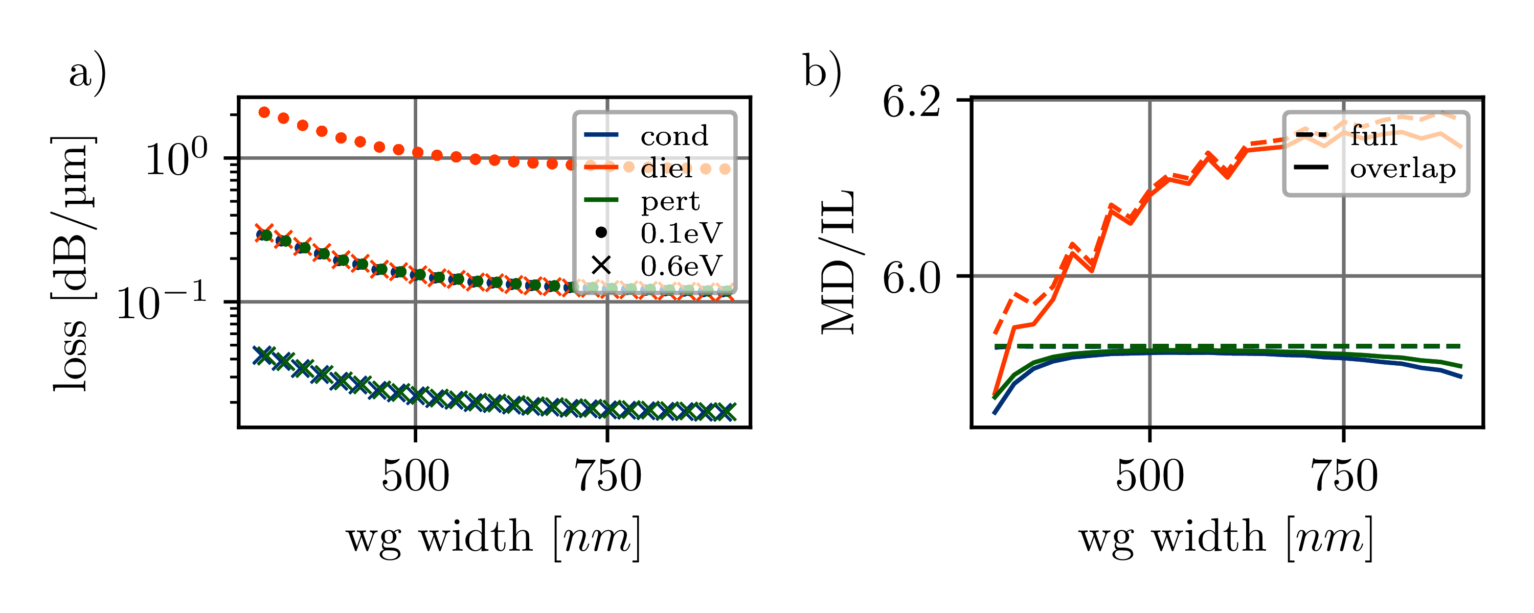
Figure 3:Graphene loss of buried silicon strip waveguides of varying width calculated using the following models: conductive boundary condition, effective dielectric layer of finite height, perturbative (see section \ref{ap:perturbation}). (a) The loss was evaluated in the on and off state with a chemical potential of \qty{0.6}{eV} and \qty{0.1}{eV} respectively (T=\qty{300}{K} and \gamma=\qty{5e13}{\per\s}). For better visibility the cond markers are shifted to the right by \qty{3}{nm} and the diel markers by \qty{6}{nm}. An overlap of \qty{2}{\micro \m} is used for demonstration. Both plots show the idealized model in which the optical properties are modulated in all graphene regions (dashed in (b)) and a more realistic model, that keeps the access regions fixed in the absorptive state (solid in (b)). The difference is indiscernible in (a) due to the logarithmic scaling. (b) The attained MD/IL ratio was extracted from (a).

Figure 4:Convergence behavior of FDE simulations of graphene introduced attenuation comparing the boundary condition method () and the effective permittivity method () at different chemical potential. The x-axis indicates the number of mesh cells in a region of \qty{5}{nm} above and below the graphene sheets, which are separated by \qty{5}{nm}.
Comparison\label{ap:comparison_loss_models}
In the following, it will be shown, that the two expressions found above are equivalent. Starting with the observation, that the denominator in equation \ref{eq:gamma_overlap} contains the surface integral over the time-averaged pointing vector . The integral thus represents the power flow perpendicular through integration plane . Thus one finds:
Comparison to equation \ref{eq:ohmic} considering that the thickness of the integration region is fixed to the effective graphene thickness :
With the expressions for and one finds:
Which is consistent with the expression in equation \ref{eq:eff_epsilon}. The two perturbative expressions for graphene absorption have thus been shown to be equivalent.
Locality of Doping and Strain\label{sec:acf}
Spatial inhomogeneity in the local doping of graphene can lead to a reduction of the effective absorption switching Mohsin et al., 2014 (more details in section Device Size with locally correlated Doping). It is thus important to quantify these variations and their topography. The variations in doping were extracted from the - and -peak positions, as described in Raman Spectroscopy, for each position on a grid rastered by the confocal microscope. From these maps the mean and standard deviation in doping, and its PDF were determined. To describe the topography of the doping surfaces the two-dimensional discrete (normalized) ACF of the doping/Fermi energy surfaces (, ) was determined by:
Where is the crosscorrelation function of and defined as (generalized from Zhao et al., 2006):
Where is the total number of pixels, and is the number of pixels from the center of the map to the edge. Direct evaluation of equation \ref{eq:crosscorr} for maps with large () pixel count is computationally intensive. It can however be sped up by considering the similarities to the convolution and leveraging the frequency domain formulation of the latter. Surface topographic features that exhibit a property analogous to the Markov property have been shown to yield an exponential autocorrelation function decaying radially with Agterberg, 1970:
Where is the radial displacement from the origin and is defined as the correlation length of the surface. To obtain in this work, was numerically averaged radially. Surfaces with exponential ACF have been observed and analyzed extensively in literature Zadehgol, 2021. It is of interest, how the influence of the doping variations changes for different device sizes with respect to the correlation length. To evaluate the switching degradation due to local doping variations independent of other degrading factors a Heavyside switching behavior was assumed. The influence of doping variations, measured at a certain gate voltage (e.g. V_g=\qty{0}{V}) was modeled by the following first-order approximation: The doping was expressed in terms of a local Dirac voltage which was assumed to be constant with changes in chemical potential for every point on the graphene sheet. It has been comprehensively shown in literature, that this approximation does not fully hold i.e. due to border traps charging and discharging, which alters the potential landscape seen by the graphene Singh & Gupta (2018)Knobloch et al. (2022). However, modeling such effects would introduce a large amount of complexity and is out of the scope of this work. From the local and a global overdrive voltage the local can be found according to equation \ref{eq:v_od}, disregarding the quantum capacitance:
and with equation \ref{eq:mu_c}:
To generate random signals which exhibit a specified autocorrelative behavior the Wiener-Khinchin theorem was leveraged, stating that for a given random signal the Fourier transform of the ACF is the PSD of Ohm & Lüke, 2014. Where the PSD is the squared magnitude of the FT of ()[1]. A spectrum can be generated to have a given PSD by taking the square root of the PSD and adding a uniformly sampled random phase :
can then be transformed to using the inverse FT. This approach can be generalized to discrete time signals using the DFT and inverse DFT, commonly implemented numerically as a FFT. For one-dimensional signals with an exponential ACF, the Wiener-Khinchin theorem yields a Lorentzian PSD, as is typically observed in Wiener processes (e.g. Brownian motion, laser phase noise)
Switching Degradation due to Doping Variations\label{ap:dop_var}
The following assumptions are made: The doping variations are normally distributed with a mean and standard deviation . The shape of the doping distribution is unaffected by the electrostatic modulation, which only shifts :
Where is the PDF of the doping distribution. Moreover, the ideal modulation behavior is modeled by a shifted and mirrored Heavyside function :
The absorption is used here to avoid confusion between the standard deviation and surface conductivity. It is noted that the derivation also holds for the conductivity at optical frequencies, which is proportional to . denotes the absorption without doping. The expectation value for evaluates to:
The approximation holds for being significantly positive. For negative the derived result holds due to symmetry. As the absolute positions of are irrelevant in this analysis the evolution of with can be described by
Evaluating the positions at which reaches and on finds:
Resulting in $\Delta\mu_{c,80\
Noise Performance Modulator
Here the expressions for will be derived for a link limited by thermal noise, shot noise, and a combination of RIN and shot noise.
Thermal Noise\label{ap:thermal_noise}
As discussed in section Sources of noise in optical links thermal noise is independent of the optical power at the detector:
Thus equation \ref{eq:q-link} becomes:
Where is abbreviated as in this section. Which can be expressed in terms of the input power to the modulator and the scalar and :
Solving for and comparing it to the power required for an ideal modulator ( and ) one finds:
Defining the ROMA. indicates the factor by which the laser power has to be increased due to the nonideal modulator .
Using equation \ref{eq:md_il_f} in its scalar form one finds and thus:
Which is shown for different in figure . The position of the maximum is found as:
the maximum achievable ROMA thus evaluates to:
Shot Noise\label{ap:shot_noise}
Similarly in the shot noise limit, one finds from equation \ref{eq:q-link} that:
Again solving for and comparing the result to the ideal modulator one thus finds:
RIN and thermal noise\label{ap:rin_power}
For a combination of thermal noise and RIN, the link quality factor is determined by:
Evaluating \ref{eq:rin_p1} for is performed as follows. The equation is brought into the form of equation \ref{eq:overview_eq} by the following substitutions:
Leading to:
This equation is solved for by squaring both sides collecting all terms but the remaining square root on one side and squaring again. By eliminating trivial solutions, that were introduced by the squaring one finds:
Introducing the values from before one finds:
from there the comparison to an ideal modulator with infinite modulation depth yields:
Singly Coupled Resonator
HWHM \label{ap:hwhm}
The HWHM in terms of phase can be found from \ref{eq:t_allpass} to be:
which was found to be approximately for close to 1 (see fig. ). This approximation is used to normalize in the following. According to \ref{eq:hwhm} the HWHM can only be determined for , as is not reached else. \begin{figure}[h] \centering \begin{subfigure}[b]{.5\linewidth} \includesvg[width=\textwidth]{HWHM_phase.svg} \caption{} \end{subfigure} \begin{subfigure}[b]{.3\linewidth} \includesvg[width=\textwidth]{HWHM_tau.svg} \caption{} \end{subfigure} \caption{The HWHM of the resonance dip in terms of for different coupler transmission (a) and its dependence on (b). An approximation to the dependence is indicated by the dashed line.} \label{fig:HWHM} \end{figure}
Offresonant IL
Figure Figure 5 shows the IL in the offresonant case.
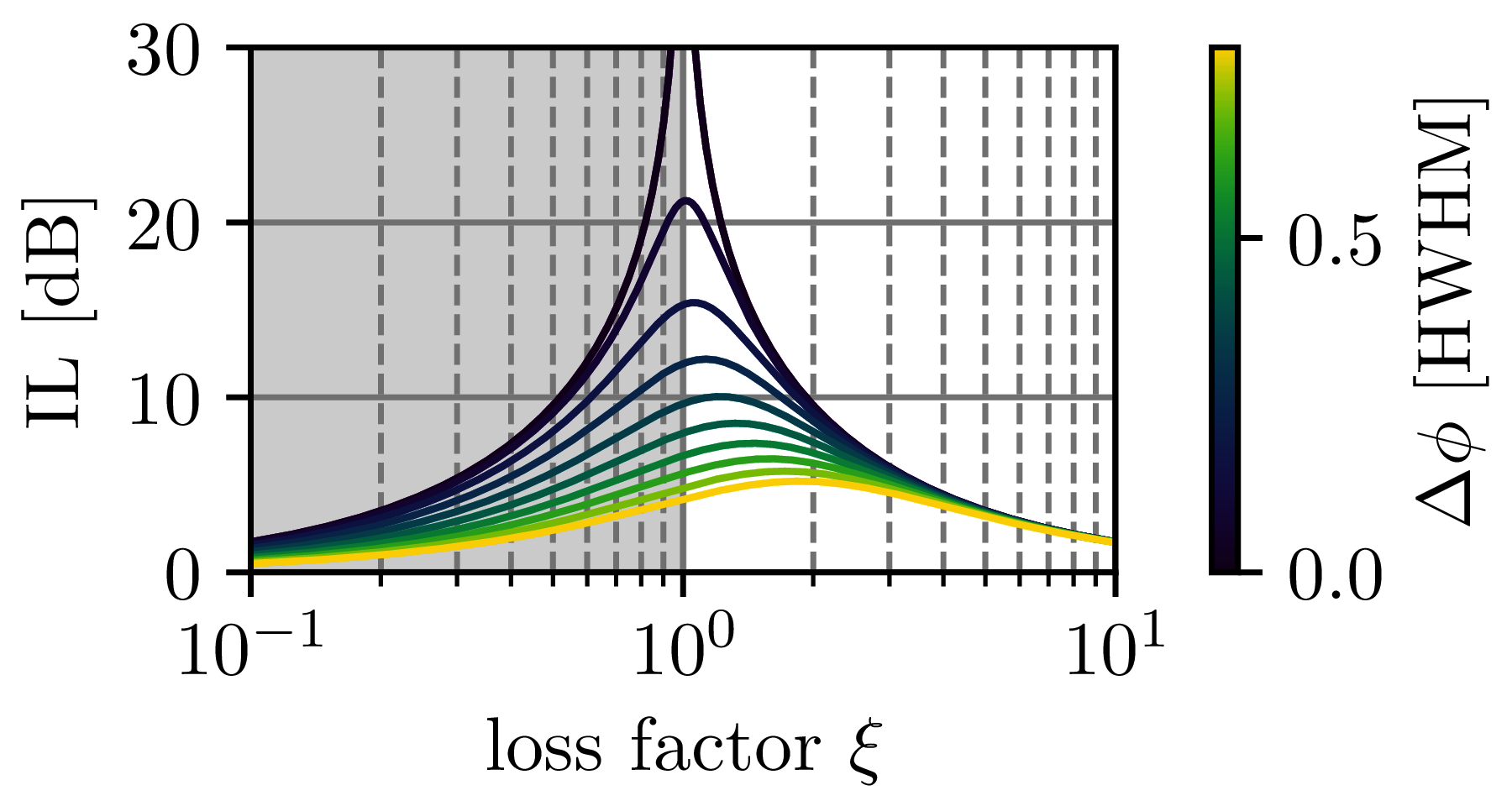
Figure 5:Reduction in IL for detuning from resonance evaluated at . With increasing detuning an asymmetry between the over- and undercoupled regime is introduced. IL improves strongly in the overcoupled case (marked in grey), while little change is observed in the undercoupled regime. This can lead to an inversion of the switching behavior between resonant and detuned wavelengths for an undercoupled modulator.
Q/V \label{ap:qv_eta}
Motivated by section Arbitrarily shaped Cavities lets assume:
Where is the required graphene length and is some proportionality constant. Solving for eta and inserting the expressions for , and one finds:
Undefined control sequence: \unit at position 69: …alpha_{trans} [\̲u̲n̲i̲t̲{dB \per \m}]} …

\eta = \frac{-20 \pi n_g}{A \lambda_{res}} \frac{d}{\alpha_{trans} [\unit{dB \per \m}]} \frac{\log_{10}(a\tau)\sqrt{a\tau}}{1-a\tau}
In the limit of large round trip transmission the latter part converges to:
The expression for thus becomes:
Undefined control sequence: \unit at position 85: …\alpha_{trans}[\̲u̲n̲i̲t̲{dB \per \m}]} …

\lim_{a\tau\to1} \eta = \frac{20 \pi n_g \log_{10}(e)}{A\lambda_{res}\alpha_{trans}[\unit{dB \per \m}]} \left[ \unit{m^{-2}}\right]
Using the approximate values presented in table \ref{tab:eta_parameters} eta is evaluated to be \eta\approx\qty{2e17}{m^{-2}}. \begin{table}[] \centering \begin{tabular}{c|cc} Property & Quantity & Unit \ \hline & 5 & - \ & 4.4 & - \ & 0.2 & \unit{\micro\m^2} \ & 1550 & nm \ \multicolumn{1}{l|}{} & \multicolumn{1}{l}{\num{1e4}} & \multicolumn{1}{l}{\unit{dB\per\m}} \end{tabular} \caption{Approximate values used to evaluate \eta\approx\qty{2e17}{m^-2}. and are based on FDE simulations of a \qtyproduct{220x500}{nm} SOI waveguide. The other quantities are chosen based on analysis in the main body of this work.} \label{tab:eta_parameters} \end{table}
Domination factor
\label{ap:domination} Given
and
note that
The reduced switching factor is described by:
with
and thus
and with
one finds
Reflective Modulator Converter \label{ap:refl_conversion}
The photonic circuit shown in Figure 6 is suitable to extract the output light from a reflective modulator. It relies on a phase shift applied to the light that couples from one waveguide to the other in a 50:50 DC. As the light transits the DC twice light ending up in the upper left waveguide has experienced this phase shift exactly once regardless of the path it took (upper or lower reflector). The light exiting at the lower left has either experienced the phase shift twice or not at all. The resulting phase difference leads to destructive interference in the lower arm, with all light interfering constructively in the upper arm. The configuration is essentially a Michelson interferometer that has arms of equal length.

Figure 6:Photonic circuit to separate the incident and reflected light from a reflecting modulator enabling its use in communication links. (a) shows a reflective modulator, which is duplicated and attached to both output waveguides of a DC (b) to separate the modulated from the incident light.
Goos Modification\label{ap:spins_mod}
The following example demonstrates how the functions generating the parametrizations were modified. The original function definition can be found here.
from discretize import TensorMesh

def compat_param(...
                 var = None,
                 #added to allow using existing variable
                 **kwargs)
    -> Tuple[goos.Variable, OldStyleParametrization]:
    '''
    ...
    '''
    _, var_shape, lower_bound, upper_bound = create_old_param(
        param, extents, pixel_size)

    if not var: #if exists use given variable
        var = goos.Variable(initializer(var_shape),
                            name=var_name,
                            lower_bounds=lower_bound,
                            upper_bounds=upper_bound)

    return var, OldStyleParametrization(var=var,
                                        ...
                                        **kwargs)
Program 1:Modification to the generation of the parametrization.
Modifications for BEOL Integration\label{ap:beol}
The planned BEOL integration poses multiple challenges to resonant graphene modulators. Due to the lacking availability of crystalline silicon in the BEOL, the waveguide material has to be replaced, resulting in the following two challenges: Most of the available dielectrics transparent at telecommunication wavelengths are non-conductive. Therefore the use of a GIG capacitor becomes mandatory. Therefore the model for the influence of doping variations should be augmented to consider correlated and uncorrelated variations in doping of the two separate sheets. Similarly, it becomes necessary to align the relative position of the idle doping level. Moreover, with the exception of amorphous silicon, the available dielectrics have drastically lower refractive index compared to silicon, resulting in a decreased index contrast and therefore confinement. The lower confinement bears two problems. It leads to an increased overlap with pads and access graphene, lowering . To compensate the overlap and pad separation have to be increased, penalizing the bandwidth. Furthermore, the lowered contrast reduces the ability to guide light, which should increase the mode volume and lower . The exact influence on the required graphene area should be modeled in further detail going forward. The larger resonator dimensions will also pose additional computational cost on the inverse design algorithm, which can be partially compensated by less demanding mesh requirements.
Miscellaneous
\input{sections/Methodology/util}
- Chrostowski, L., & Hochberg, M. (2015). Silicon Photonics Design: From Devices to Systems. Cambridge University Press. 10.1017/CBO9781316084168
- Romero-García, S., Merget, F., Zhong, F., Finkelstein, H., & Witzens, J. (2013). Silicon Nitride CMOS-compatible Platform for Integrated Photonics Applications at Visible Wavelengths. Optics Express, 21(12), 14036. 10.1364/OE.21.014036
- Zhang, Y., Yang, S., Lim, A. E.-J., Lo, G.-Q., Galland, C., Baehr-Jones, T., & Hochberg, M. (2013). A Compact and Low Loss Y-junction for Submicron Silicon Waveguide. Optics Express, 21(1), 1310. 10.1364/OE.21.001310
- De la Cruz-Coronado, J. M., Prosopio-Galarza, R., & Rubio-Noriega, R. E. (2020). Silicon Photonics Foundry-oriented Y-junction Optimization. 2020 IEEE XXVII International Conference on Electronics, Electrical Engineering and Computing (INTERCON), 1–4. 10.1109/INTERCON50315.2020.9220205
- Joannopoulos, J. D. (Ed.). (2008). Photonic Crystals: Molding the Flow of Light (2nd ed). Princeton University Press.